
Huawei pitches τ scaling with LogicFolding and a 1.4nm-equivalent 2031 target
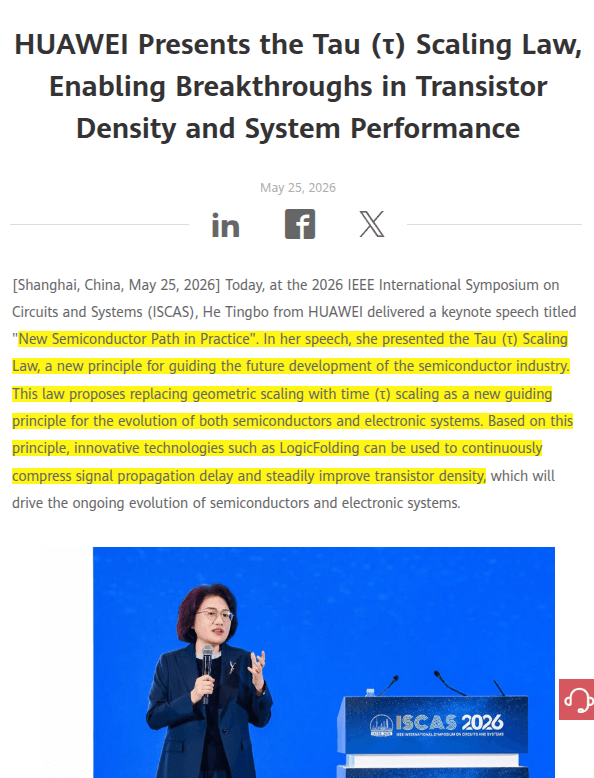
Huawei outlined a τ scaling framework and LogicFolding design that shifts chip progress from node shrinkage toward shorter signal delay. The proposal matters because it targets performance, density, and yield gains without relying only on EUV-era process shrinks.
TL;DR
- In a Huawei announcement, the company pitched a new τ scaling framework that treats signal delay, not transistor geometry alone, as the main optimization target across devices, circuits, chips, and systems, a framing echoed by rohanpaul_ai's summary and WesRoth's overview.
- Huawei says 381 chips have already been designed and mass-produced under this approach, while WesRoth's post says fall 2026 Kirin chips will be the first public test of the LogicFolding piece of that stack.
- According to the paper abstract, LogicFolding is paired with system-level work including UnifiedBus and Hi-ONE optical I/O, so the pitch is much broader than a single packaging trick.
- The headline 2031 target, which rohanpaul_ai and kimmonismus both describe as 1.4nm-class or 14Å-class density, is easy to overread: ZhihuFrontier's technical review argues the claim is package-footprint density equivalence, not full process-node parity on frequency, energy, or cost.
- The most credible part of the public material is not the slogan but the bottleneck list, because ZhihuFrontier's earlier thread and its longer follow-up both stress EDA, yield, clock skew, and vertical interconnect tradeoffs that still have to work in real silicon.
You can read Huawei's own announcement and the linked paper abstract, and the weirdest reveal is how much of the story is really about wiring, clocking, and packaging instead of transistor shrink. The public summaries also surface concrete subsystem names, including LogicFolding, SkyBridge, SkyClock, UnifiedBus, and Hi-ONE, with ZhihuFrontier's thread and the longer breakdown doing most of the heavy lifting on what those names are supposed to mean.
τ scaling
Huawei's core claim is simple: Moore-era gains increasingly came from reducing total delay, so future scaling should optimize delay directly across the whole machine, not only through smaller transistors. That is the framing in Huawei's own announcement, and rohanpaul_ai's LogicFolding explainer restates it as a shift from asking how small the transistor is to asking where time is being lost.
The stack Huawei is describing has at least three layers:
- Circuit level: LogicFolding tries to shorten critical wires and reduce parasitic delay, according to rohanpaul_ai's explainer.
- Chip level: Huawei says hardware, architecture, and software are being co-designed to improve instruction and data flow, per WesRoth's summary.
- System level: UnifiedBus is meant to reduce communication latency across larger computing systems, again according to WesRoth's summary.
The catchy part is the slogan. The useful part is that Huawei is trying to give process, packaging, architecture, and software teams one shared metric.
LogicFolding
LogicFolding is the concrete engineering hook inside the broader τ story. In rohanpaul_ai's explainer, the idea is vertical proximity: place logic that needs to communicate above and below itself instead of spreading it across a flat die, so important signals travel less distance.
The public commentary around the slides breaks that into a few specific mechanisms:
- SkyBridge: a routing scheme that uses horizontal and vertical paths, with top metal layers carrying fast data paths, according to ZhihuFrontier's thread.
- SkyClock: top-down clock distribution with post-silicon skew adjustment, which ZhihuFrontier's thread says is unusual for fixed ASIC-style designs.
- Hybrid bonding and TSV-scale interconnects: ZhihuFrontier's longer review frames the implementation as sub-2 μm hybrid bonding plus cross-die logic partitioning and custom EDA.
That makes the announcement feel less like a new law of physics and more like a branded 3D-integration program with a unifying metric attached.
Density claims
The loudest number in circulation is the 2031 density target. rohanpaul_ai's report says Huawei is aiming for 1.4nm-class density by 2031, while kimmonismus presents that as a way to close the gap without EUV.
The caveat is that Huawei's public framing appears to mix several different kinds of equivalence. In ZhihuFrontier's longer review, the density math is described as package-footprint density that counts stacked active tiers in one footprint. That is a real packaging metric, but it is not the same as saying Huawei will match a leading-edge foundry node across frequency, energy efficiency, yield, and cost.
That same review also says the most eye-catching LogicFolding numbers, including +55% density, +41% energy efficiency, and +13% frequency at the same node, were presented without die photos, wafer-level yield curves, full PPA baselines, or workload and test-condition detail. The right reading, based on the material now public, is that Huawei has shown a direction and a roadmap, not audited silicon proof.
Yield and EDA
The most interesting technical detail is not the 2031 slogan. It is that Huawei's own public narrative, as relayed by ZhihuFrontier's early thread and the longer review, repeatedly comes back to yield tolerance and toolchain limits.
SkyClock is a good example. ZhihuFrontier's early thread says Huawei is talking about post-silicon clock-skew adjustment, which trades area and power overhead for tolerance to process variation. That trade matters more if the manufacturing node is older or less stable, because more chips can be trimmed back into spec instead of binned down or thrown away.
The same thread and follow-up review list the hard parts plainly:
- 3D-native EDA: placement, timing closure, parasitics, and keep-out-zone modeling across stacked dies, per ZhihuFrontier's longer review.
- Cross-wafer variation: bonded wafers can bring larger Vth, drive-current, and RC differences than one-die timing flows expect, again per that review.
- Vertical interconnect cost: every bond and TSV adds its own resistance and capacitance, so folding only works when the delay benefit exceeds the delay penalty, according to the same source.
- Thermals: teortaxesTex's cooling question highlights the obvious unresolved problem for stacked active logic, even though the public material does not answer it.
Those constraints are why the story is interesting. Huawei is not only claiming more performance from packaging, it is effectively claiming a workable design flow and yield strategy around packaging.
UnifiedBus and Hi-ONE
The paper pitch is broader than smartphones. In ZhihuFrontier's review, Huawei's system roadmap extends τ scaling to AI infrastructure through UnifiedBus, near-package optical I/O under the Hi-ONE name, and a larger 3D-folding story about escaping the usual perimeter bottlenecks of 2.5D packages.
Three claims stand out:
- UnifiedBus: remote access latency is described as dropping from tens of microseconds to roughly 100 ns, although ZhihuFrontier's review argues that baseline is favorable and the 100 ns figure is ambiguous without a clearer distance scope.
- Hi-ONE optical I/O: the same review says Huawei is talking about 8 Tb/s-class near-package optical links and much shorter electrical SerDes paths before handing off to optics.
- N² vs N packaging argument: compute scales with area, but power delivery and I/O arrive from the perimeter, so 3D stacking, backside power, bonded memory, and optical links are being presented as ways to move constrained resources off the edge and onto the surface, according to the review.
That last point introduces the final useful fact in the story: Huawei is pitching τ scaling as a capital-allocation thesis as much as a chip-design thesis. In ZhihuFrontier's summary of the paper, the line is that the next dollar should follow τ, not nodes, which is a neat way to say the company wants advanced packaging, interconnect, memory proximity, and system fabrics to matter as much as lithography in the next round of semiconductor competition.